- 您现在的位置:买卖IC网 > Sheet目录1998 > ICS844021BGI-01LFT (IDT, Integrated Device Technology Inc)IC CLOCK GEN ETHERNET 8-TSSOP
IDT / ICS LVDS CLOCK GENERATOR
9
ICS844021BGI-01 REV. A NOVEMBER 6, 2012
ICS844021I-01
FEMTOCLOCKS CRYSTAL-TO-LVDS CLOCK GENERATOR
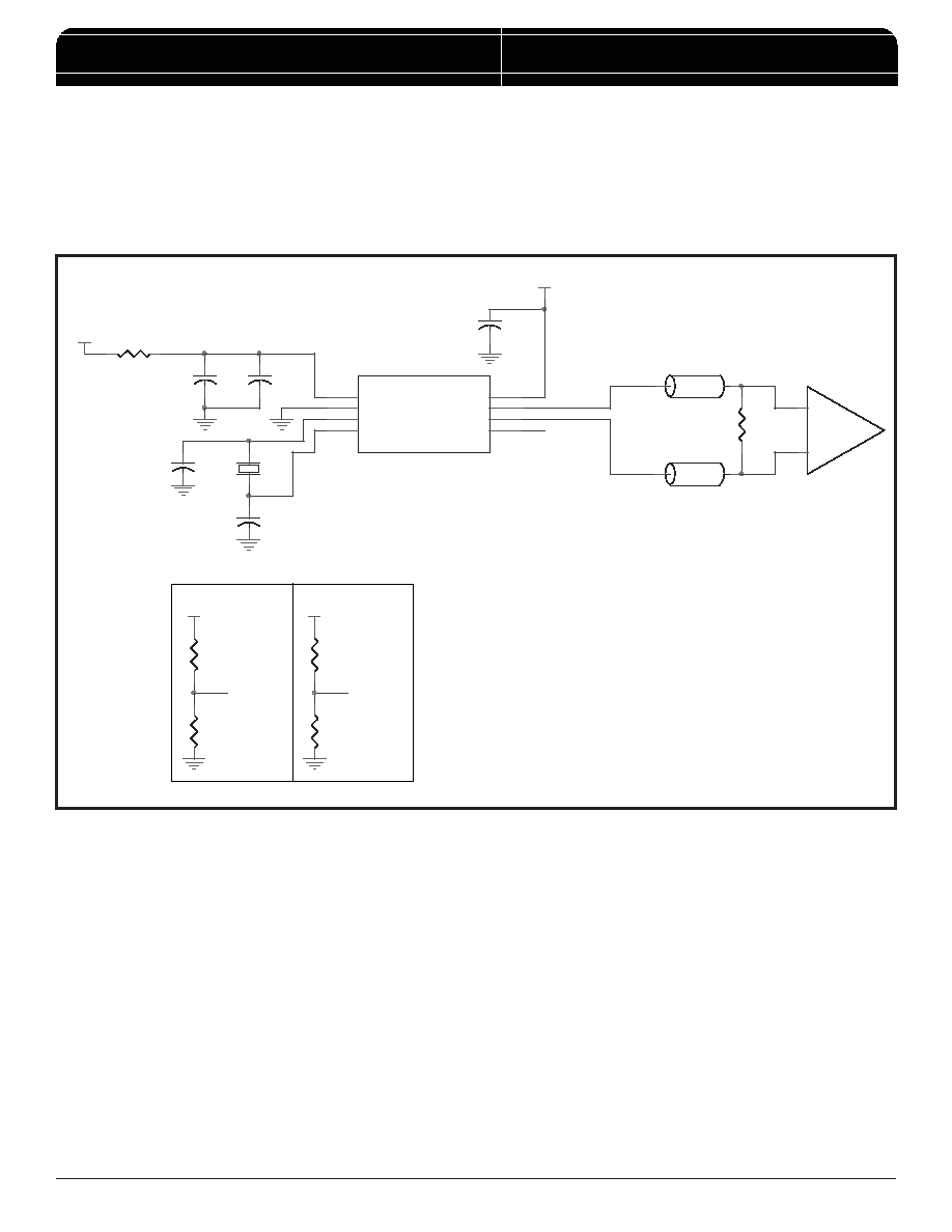
SCHEMATIC LAYOUT
Figure 5 shows an example of ICS844021I-01 application
schematic. In this example, the device is operated at V
DD
= 3.3V.
The decoupling capacitor should be located as close as
possible to the power pin. The 18pF parallel resonant 25MHz
crystal is used. The C1 = 33pF and C2 = 27pF are recommended
U1
ICS844021I-01
1
2
3
4
8
7
6
5
VDDA
GND
XTAL_OUT
XTAL_IN
VDD
Q0
nQ0
OE
C1
33pF
1 8 p F
nQ
+
-
VDD
Zo = 50 Ohm
X1
25 MHz
R2
100
C4
10u
OE
Zo = 50 Ohm
RU2
Not Install
VDD
RD1
Not Install
To Logic
Input
pins
RU1
1K
R1
10
C3
0.1u
Set Logic
Input to
'1'
Logic Input Pin Examples
Q
C5
0.01u
To Logic
Input
pins
C2
27pF
Set Logic
Input to
'0'
RD2
1K
VDDA
VDD
for frequency accuracy. For different board layout, the C1 and
C2 may be slightly adjusted for optimizing frequency accuracy.
For the LVDS output drivers, place a 100
Ω resistor as close to
the receiver as possible.
FIGURE 5. ICS844021I-01 SCHEMATIC LAYOUT
发布紧急采购,3分钟左右您将得到回复。
相关PDF资料
ICS844071AGLFT
IC CLOCK GEN GIG ETH 8-TSSOP
ICS844201BG-45LF
IC CLK GENERATOR 25MHZ 8TSSOP
ICS844204BK-245LF
IC CLK SYNTHESIZER 4LVDS 32VFQFN
ICS844S42BKILF
IC SYNTHESIZER RF FREQ 56-VFQFPN
ICS86004BG-01LF
IC CLK BUFFER ZD 1:4 16-TSSOP
ICS8634BY-01LFT
IC BUFFER ZD 1-5 LVPECL 32-LQFP
ICS8701AY-01LF
IC CLK GEN POLARITY CTRL 48-LQFP
ICS8701CYLF
IC CLK GENERATOR /1 /2 48-LQFP
相关代理商/技术参数
ICS8440258AK-46LF
功能描述:IC SYNTHESIZER 8OUTPUT 32-VFQFPN RoHS:是 类别:集成电路 (IC) >> 时钟/计时 - 时钟发生器,PLL,频率合成器 系列:HiPerClockS™, FemtoClock™ 标准包装:1,000 系列:- 类型:时钟/频率合成器,扇出分配 PLL:- 输入:- 输出:- 电路数:- 比率 - 输入:输出:- 差分 - 输入:输出:- 频率 - 最大:- 除法器/乘法器:- 电源电压:- 工作温度:- 安装类型:表面贴装 封装/外壳:56-VFQFN 裸露焊盘 供应商设备封装:56-VFQFP-EP(8x8) 包装:带卷 (TR) 其它名称:844S012AKI-01LFT
ICS8440258AK-46LFT
功能描述:IC SYNTHESIZER 8OUTPUT 32-VFQFPN RoHS:是 类别:集成电路 (IC) >> 时钟/计时 - 时钟发生器,PLL,频率合成器 系列:HiPerClockS™, FemtoClock™ 标准包装:1,000 系列:- 类型:时钟/频率合成器,扇出分配 PLL:- 输入:- 输出:- 电路数:- 比率 - 输入:输出:- 差分 - 输入:输出:- 频率 - 最大:- 除法器/乘法器:- 电源电压:- 工作温度:- 安装类型:表面贴装 封装/外壳:56-VFQFN 裸露焊盘 供应商设备封装:56-VFQFP-EP(8x8) 包装:带卷 (TR) 其它名称:844S012AKI-01LFT
ICS8440258AKI-46LF
功能描述:IC SYNTHESIZER 8OUTPUT 32-VFQFPN RoHS:是 类别:集成电路 (IC) >> 时钟/计时 - 时钟发生器,PLL,频率合成器 系列:HiPerClockS™, FemtoClock™ 标准包装:27 系列:Precision Edge® 类型:频率合成器 PLL:是 输入:PECL,晶体 输出:PECL 电路数:1 比率 - 输入:输出:1:1 差分 - 输入:输出:无/是 频率 - 最大:800MHz 除法器/乘法器:是/无 电源电压:3.135 V ~ 5.25 V 工作温度:0°C ~ 85°C 安装类型:表面贴装 封装/外壳:28-SOIC(0.295",7.50mm 宽) 供应商设备封装:28-SOIC 包装:管件
ICS8440258AKI-46LFT
功能描述:IC SYNTHESIZER 8OUTPUT 32-VFQFPN RoHS:是 类别:集成电路 (IC) >> 时钟/计时 - 时钟发生器,PLL,频率合成器 系列:HiPerClockS™, FemtoClock™ 标准包装:1,000 系列:- 类型:时钟/频率合成器,扇出分配 PLL:- 输入:- 输出:- 电路数:- 比率 - 输入:输出:- 差分 - 输入:输出:- 频率 - 最大:- 除法器/乘法器:- 电源电压:- 工作温度:- 安装类型:表面贴装 封装/外壳:56-VFQFN 裸露焊盘 供应商设备封装:56-VFQFP-EP(8x8) 包装:带卷 (TR) 其它名称:844S012AKI-01LFT
ICS8440259AK-05LF
功能描述:IC SYNTHESIZER 9OUTPUT 32-VFQFPN RoHS:是 类别:集成电路 (IC) >> 时钟/计时 - 时钟发生器,PLL,频率合成器 系列:HiPerClockS™, FemtoClock™ 标准包装:1,000 系列:- 类型:时钟/频率合成器,扇出分配 PLL:- 输入:- 输出:- 电路数:- 比率 - 输入:输出:- 差分 - 输入:输出:- 频率 - 最大:- 除法器/乘法器:- 电源电压:- 工作温度:- 安装类型:表面贴装 封装/外壳:56-VFQFN 裸露焊盘 供应商设备封装:56-VFQFP-EP(8x8) 包装:带卷 (TR) 其它名称:844S012AKI-01LFT
ICS8440259AK-05LFT
功能描述:IC SYNTHESIZER 9OUTPUT 32-VFQFPN RoHS:是 类别:集成电路 (IC) >> 时钟/计时 - 时钟发生器,PLL,频率合成器 系列:HiPerClockS™, FemtoClock™ 标准包装:1,000 系列:- 类型:时钟/频率合成器,扇出分配 PLL:- 输入:- 输出:- 电路数:- 比率 - 输入:输出:- 差分 - 输入:输出:- 频率 - 最大:- 除法器/乘法器:- 电源电压:- 工作温度:- 安装类型:表面贴装 封装/外壳:56-VFQFN 裸露焊盘 供应商设备封装:56-VFQFP-EP(8x8) 包装:带卷 (TR) 其它名称:844S012AKI-01LFT
ICS8440259AK-45LF
功能描述:IC SYNTHESIZER 9OUTPUT 32-VFQFPN RoHS:是 类别:集成电路 (IC) >> 时钟/计时 - 时钟发生器,PLL,频率合成器 系列:HiPerClockS™, FemtoClock™ 标准包装:1,000 系列:- 类型:时钟/频率合成器,扇出分配 PLL:- 输入:- 输出:- 电路数:- 比率 - 输入:输出:- 差分 - 输入:输出:- 频率 - 最大:- 除法器/乘法器:- 电源电压:- 工作温度:- 安装类型:表面贴装 封装/外壳:56-VFQFN 裸露焊盘 供应商设备封装:56-VFQFP-EP(8x8) 包装:带卷 (TR) 其它名称:844S012AKI-01LFT
ICS8440259AK-45LFT
功能描述:IC SYNTHESIZER 9OUTPUT 32-VFQFPN RoHS:是 类别:集成电路 (IC) >> 时钟/计时 - 时钟发生器,PLL,频率合成器 系列:HiPerClockS™, FemtoClock™ 标准包装:1,000 系列:- 类型:时钟/频率合成器,扇出分配 PLL:- 输入:- 输出:- 电路数:- 比率 - 输入:输出:- 差分 - 输入:输出:- 频率 - 最大:- 除法器/乘法器:- 电源电压:- 工作温度:- 安装类型:表面贴装 封装/外壳:56-VFQFN 裸露焊盘 供应商设备封装:56-VFQFP-EP(8x8) 包装:带卷 (TR) 其它名称:844S012AKI-01LFT